Recently, a research team led by Prof. Wenping Hu and Dr. Xiaochen Ren from Tianjin University’s School of Science reported a facile solution-printing method to fabricate centimeter-sized highly aligned organic crystalline arrays with a thickness of a few molecular layers, which was published onAdvanced Materialsunder the title of “Solution-Processed Centimeter-Scale Highly Aligned Organic Crystalline Arrays for High-Performance Organic Field-Effect Transistors”.
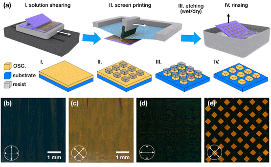
a) The schematic drawing of the procedures of solution‐processed printing and patterning of large‐area organic highly crystalline array. POM images of solution‐sheared highly crystalline film of C8‐BTBT: b) 0°, c) 45°. POM images of OSC array of C8‐BTBT: d) 0°, e) 45°. The side length of the square shape in (d) and (e) is 150 µm.
Organic single crystalline films fabricated by solution printing offer great potential for realizing large-scale, low-cost, high-performance flexible electronics as well as for fundamental materials studies.
To progress the practical utilization of organic semiconductors, there are two major issues that must be overcome. One is that the organic semiconductor thin films must be patterned without involving photolithography to reduce crosstalk between neighboring devices. The other is that the organic single crystal patterns must align crystal orientations to ensure good device uniformity, because the electrical performance of single crystal devices is highly anisotropic.
Although various solution printing methods, such as inkjet printing, gravure printing, and screen printing, have been developed to fabricate high performance OFET (organic field-effect transistor)arrays, it is difficult to find cases that overcome both of the above-mentioned issues.
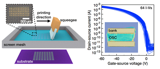
Left: schematic drawing of screen printing setup, the enlarged image is the optical image of screen mesh.
Right: I-V characteristics of 64 transistors, the inset is the optical image of screen printed device.
The research team focused on thesolution-printed organic semiconductor films and made some breakthroughs.
By employing cross-linkedorganic polymer banks to constrain the OSC (organic semiconductor) crystallization, the team realized scalable fabrication of highly crystalline organic semiconductor thin film by screen printing toward the low-cost fabrication of high-performance transistor arrays for the first time as shown in figure 1, (Adv. Mater.2019,31, 1807975).
To control over the crystallographic orientation, crystal uniformity, and thickness, they proposed a strategy to fabricate centimeter-scale highly aligned organic crystalline arrays for high-performance organic field-effect transistors(Adv. Mater.2020,32, 1908388).The solution shearing technique is used to produce large-area highly aligned organic crystalline thin film. Subsequently, the aqueous resist is screen printed on the hydrophobic surface of organic crystalline film to selectively protect it followed by wet/dry etching. The addition of surfactant in aqueous resist dramatically changes the fluid drying dynamics and increases the adhesion of the aqueous solution to the underlying non-wetting organic crystalline film. As a result, centimeter-scale organic crystalline arrays are successfully prepared on different substrates.This method is a key step to build sophisticated organic integrated circuits and to realize the full‐printing of high‐performance organic electronics.
Link to the paper:https://doi.org/10.1002/adma.201908388
By the School of Science
Editor: Eva Yin
